해당 글은 imec의 을 번역한 글입니다.
References
- ‘Towards a process flow for monolithic CFET transistor architectures,’ imec reading room
- ‘Monolithic complementary field effect transistors (CFET) demonstrated using middle dielectric isolation and stacked contacts,’ S. Demuynck et al., VLSI 2024
- ‘Monolithic-CFET with direct backside contact to source/drain and backside dielectric isolation,’ A. Vandooren et al., IEDM 2024
- ‘Imec proposes double-row CFET for the A7 technology node,’ imec press release
- ‘Multi-node scaling potential of monolithic CFET,’ S. Yang et al., IEDM 2025
- ‘Outer wall forksheet to bridge nanosheet and CFET device architectures in the logic technology roadmap,’ imec reading room
- ‘Hybrid channel monolithic-CFET with Si (110) pMOS and (100) nMOS,’ A. Vandooren et al., IEDM 2025
1. Introduction
CFET(Complementary FET) 소자 아키텍처는 로직 기술 로드맵에서 GAA(Gate-All-Around) 나노시트 트랜지스터의 후계자로 자리잡을 것으로 예상된다. CFET 소자에서는 nMOS와 pMOS 트랜지스터가 수직으로 적층되어, n-p 간격을 표준 셀 높이 계산에서 제외할 수 있게 된다. 이러한 구조적 특성 덕분에 CFET 소자 아키텍처는 로직 표준 셀 크기를 대폭 줄일 수 있는 잠재력을 가지고 있다. 단, 이를 실현하려면 트랜지스터의 컨택(contact) 형성 및 전원 공급을 위한 첨단 기술과의 결합이 전제되어야 한다.
모든 가능한 공정 통합 방식 중에서, monolithic CFET(mCFET)은 가장 least disruptive 방식으로 평가된다. Monolithic 공정 통합 방식에서는 공통 상단 게이트와 하단 게이트를 가지는 수직 소자 구조가 단일한 연속 공정 단계를 통해 패터닝되고 처리된다.
층의 수직 적층은 여러 가지 챌린지를 수반하며, 스택 단면의 핵심 부위에서 수직 방향의 절연을 구현하기 위해 CFET 전용 모듈이 필요하다. 그 대표적인 예가 중간 유전체 절연(MDI, Middle Dielectric Isolation) 모듈로, 상단 게이트와 하단 게이트 사이의 절연을 제공한다 [1]. 이를 통해 상단 소자와 하단 소자에 서로 다른 문턱 전압(threshold voltage)을 설정할 수 있다.
최근 몇 년간 300mm mCFET 공정 통합 플로우를 위한 핵심 빌딩 블록을 실증하는 데 있어 상당한 진전이 이루어졌다. VLSI 2024에서 imec 연구진은 MDI 모듈을 갖춘 mCFET 소자를 보고했으며, 이는 게이트와 소스/드레인(S/D)을 절연하는 나노시트 고유의 구조인 이너 스페이서(inner spacer)와 호환되는 것이었다 [2]. IEDM 2024에서는 하단 pMOS 소자의 S/D에 대한 직접 후면 컨택(direct backside contact)을 갖춘 동작 가능한 mCFET을 실험적으로 시연했다 [3].
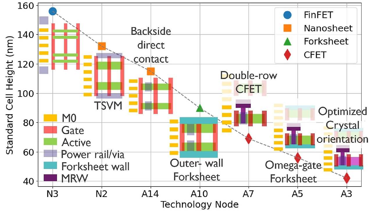
imec은 mCFET 소자 아키텍처가 로직 기술 로드맵의 A7 노드에서 도입될 것으로 전망하고 있으며, 이 시점에서 mCFET이 외벽 포크시트를 대체하게 될것으로 예상된다. 외벽 포크시트는 mCFET의 양산 준비가 완료되기 전까지, 나노시트 기반 로직 로드맵을 A10 노드까지 연장하는 역할을 담당할 것으로 구상되고 있다.

2. Extendibility of mCFET to further nodes: an industry concern
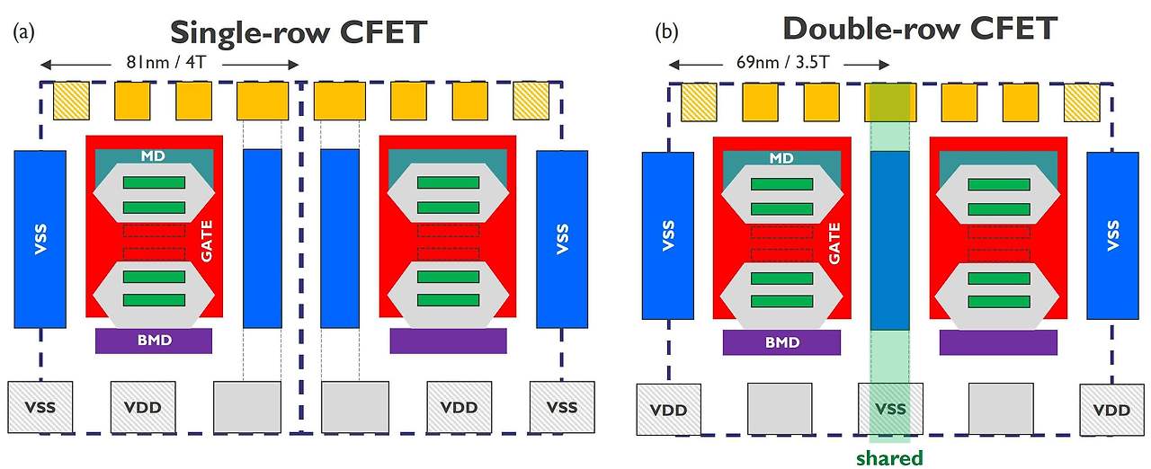
회로 레벨에서 imec은 이중 행 CFET(double-row CFET) 아키텍처를 mCFET을 A7 표준 셀에 통합하는 가장 최적의 방식으로 제안했다 [4]. 이중 행 CFET 표준 셀은 두 행의 수직 적층 소자로 구성되며, 그 사이에 공유 수직 신호 비아(shared vertical signal via)가 배치되고, 셀 경계에는 'VSS' 전원 벽(power wall)이 위치한다. IEDM 2024에서 imec은 DTCO(설계-기술 공동 최적화) 연구를 통해, 이 이중 행 CFET 아키텍처가 A7 기술 노드에서 제조 가능성과 면적 효율성 사이의 최적 트레이드오프를 제공함을 입증했다.
그러나 업계는 새로운 소자 아키텍처로의 전환을 항상 꺼려왔다. 이는 막대한 장비 투자와 추가적인 리스크를 수반하기 때문이다. 전환이 성공적으로 이루어지려면, 새로운 아키텍처가 여러 세대의 노드에 걸쳐 지속적으로 활용될 수 있어야 한다는 점이 중요하다. 이에 imec 연구진은 이중 행 mCFET의 후속 기술 노드로의 확장 가능성(scalability)을 검토하기 위해 DTCO 연구를 이어갔다.
회로 레벨에서 PPA 지표를 평가하기 위해, 15단 링 오실레이터(즉, mCFET 기반 인버터 15개로 구성된 RO)의 동작을 시뮬레이션했다. 해당 RO는 A7, A5, A3 노드 사양에 맞춰 점점 더 작아지는 표준 셀 레이아웃으로 구현되었다. 확장 가능성을 뒷받침하려면, 전력 밀도 예산이 제한된 조건 하에서 노드가 전환되더라도 RO의 성능이 유지되어야 한다. 성능 평가의 핵심 지표는 RO의 동작 주파수로, 유효 구동 전류와 유효 커패시턴스의 비($I_\mathrm{eff}/C_\mathrm{eff}$)로 표현된다.
3. 기생 커패시턴스 최적화, 포크시트 아키텍처, M0 전원 레일, 하이브리드 채널: 핵심 성능 부스터
표준 셀 치수가 축소됨에 따라 개별 CFET 채널의 나노시트 폭도 함께 감소하여, 유효 구동 전류가 낮아지고 기생 커패시턴스가 증가한다. 따라서 이러한 파라미터들의 균형을 맞추고 전력 밀도 상승을 억제하면서 노드 간 동등한 성능을 유지하기 위해 성능 부스터가 필요하다. 2025년 IEDM에서 발표된 DTCO 연구는 면적 스케일링 목표를 달성하기 위해 각 노드에서 어떤 부스터가 필요한지를 밝히고 있다 [5].
A7 노드에서는 게이트 기생 커패시턴스를 추가로 최소화함으로써 N2 나노시트 노드에 필적하는 RO 성능을 달성할 수 있다. 이는 게이트 면적과 게이트를 향하는 도체 면적을 줄임으로써 구현 가능하다. 선택적으로, 이중 행 CFET의 전원 벽을 MOL(Middle of Line)로 이동하여 M0 전원 레일로 전환하면 추가적인 이점을 얻을 수 있다.
A5 노드로의 스케일링에는 외벽 포크시트 소자 아키텍처의 도입이 필요하다. 지금까지 포크시트 아키텍처는 나노시트형 소자의 연장선으로 제안되어 왔으나 [6], 그 구조는 CFET 설계와도 완전히 호환된다. 외벽 포크시트의 특징인 wall-last 방식은 채널 스트레인을 향상시켜 CFET 소자의 구동 전류를 높인다는 점에서 주목된다. 포크시트의 공유 n-n 또는 p-p 벽에 의해 허용되는 더 작은 게이트 확장부(gate extension)는 게이트 기생 커패시턴스를 줄여준다. 나아가 채널을 보다 효과적으로 감싸는 오메가(Ω)형 게이트를 구현하면 더욱 큰 이점을 얻을 수 있다.
A3 노드에서는 오메가(Ω)형 게이트 외벽 포크시트와 M0 전원 레일에 더해 추가적인 성능 부스터가 필요하다. 유효 구동 전류는 하이브리드 채널 방향(hybrid channel orientations)을 도입함으로써 더욱 향상시킬 수 있다. 채널 방향을 조정하면 캐리어 이동도에 영향을 미치는데, 최적의 방향은 n형과 p형 소자에 따라 서로 다르다. 또한 최적의 선택은 채널에 스트레인이 도입되는지 여부와 그 크기에 따라서도 달라진다는 점에 유의해야 한다. imec 연구진은 다양한 채널 방향 조합을 평가하였으며, 가장 최적의 조합은 구동 전류를 최대 20%까지 향상시키는 것으로 나타났다. 이에 수반되는 전력 밀도 증가는 채널 폭을 조절하여 상쇄할 수 있다.

4. Embedded MDI module opens doors to hybrid channel orientations in an A3 mCFET process flow
At IEDM 2025, imec has experimentally demonstrated the key module that allows integrating channels with different orientations for the top nMOS and bottom pMOS devices in a mCFET process flow: the embedded MDI module [7].
The process flow for creating the eMDI starts with a carrier and a donor wafer on which the CFET-specific stacks of Si and sacrificial SiGe layers are grown epitaxially, for the bottom and top channels respectively. These epitaxial stacks are then recombined using wafer fusion bonding. The SiCN bonding dielectric becomes the embedded MDI single film of the mCFET device architecture, isolating the bottom and top parts. After these steps, processing of the mCFET is completed using the conventional mCFET flow, including nanosheet patterning, Si fin reveal, gate and inner spacer formation, bottom and top S/D epitaxy, and replacement metal gate.
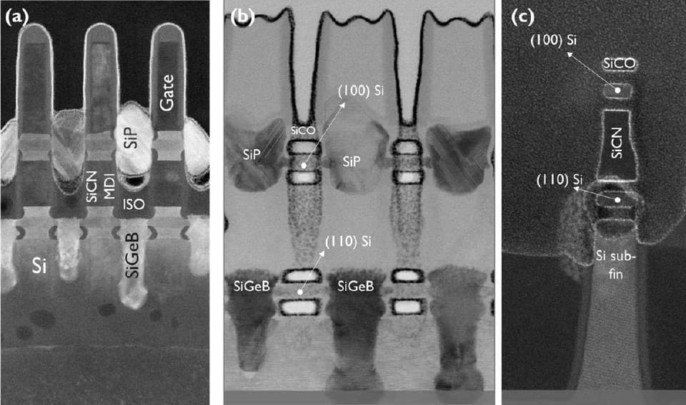
Figure 5 – TEM cross-sections of mCFET with eMDI module and top (100) Si channel and (110) bottom channel (as presented at IEDM 2025).
Imec successfully integrated this eMDI module in a full mCFET flow, and demonstrated functional top devices with various channel orientations: (100) Si top nFETs, (100) and (110) Si top pFETs. The top devices were fabricated with frontside connectivity.

Figure 6 – SiCN MDI layer transfer with hybrid nanosheet channels featuring top (100) Si orientation and bottom (110) Si orientation: (a) TEM and (b) high-resolution TEM cross-sections and (c) Fast Fourier Transform confirming the 2 different crystal orientations (as presented at IEDM 2025).
The integration flow was then extended with direct backside contacting to the mCFET bottom device. The imec CFET team demonstrated functional mCFET devices with integrated eMDI module, (100) Si top nFET connected from the frontside, and (110) Si pFET with direct backside contact.
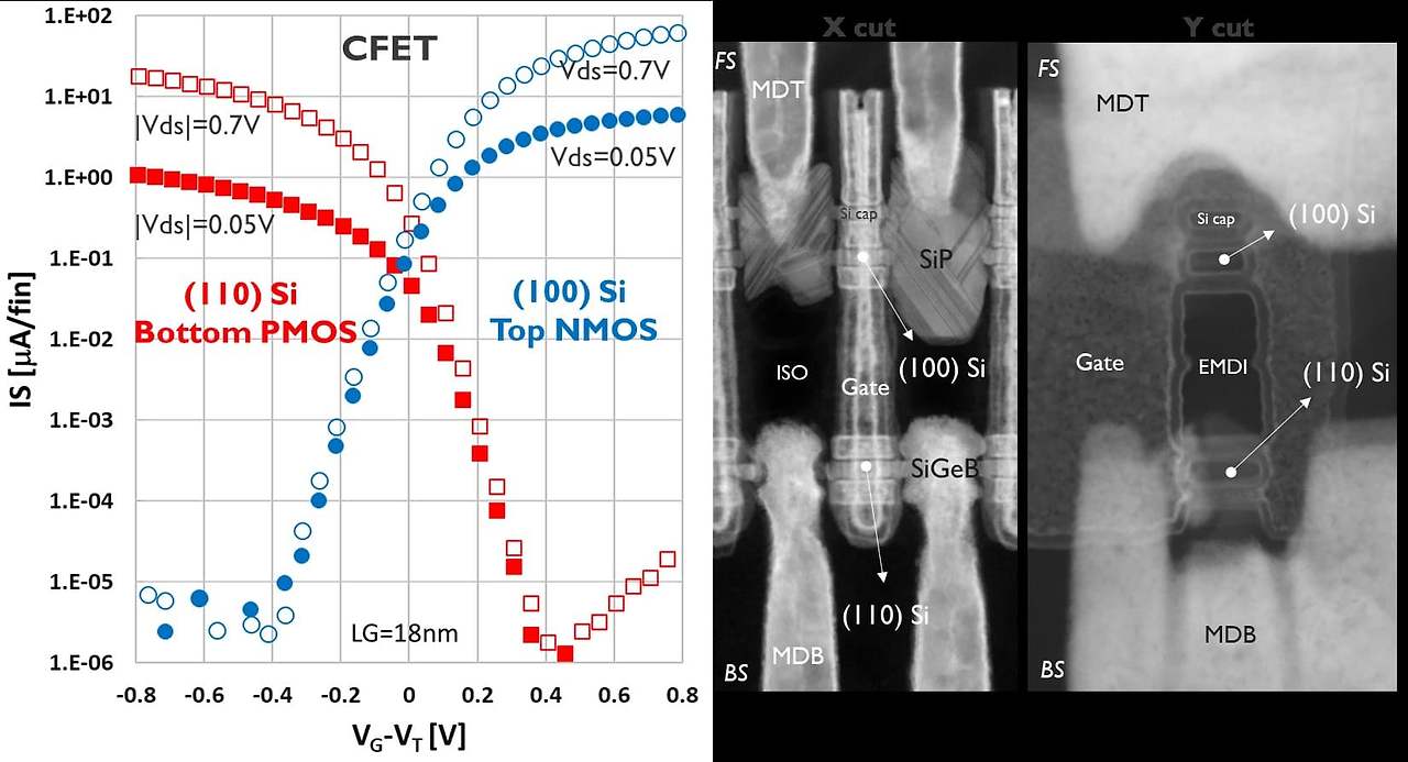
Figure 7 – (Left) Id/Vg curves and (right) TEM cross sections of mCFET with eMDI module, (100) Si top nFET, and backside contacted (110) Si bottom pFET.
Benefits of eMDI: heterogeneous channels, simplified MDI process flow, simpler Si/SiGe epi growth, more stacked Si channels
The eMDI module has several benefits compared to an earlier flavor of the MDI module, referred to by imec as the replacement MDI or rMDI [1]. With rMDI, the active Si/SiGe epi stack is turned into one tall Si/SiGe1/SiGe2 multilayer stack. Later in the process flow, the sacrificial SiGe1 layers are replaced with the gate’s work function metals, and the Ge-rich SiGe2 layers are converted into the MDI dielectric.
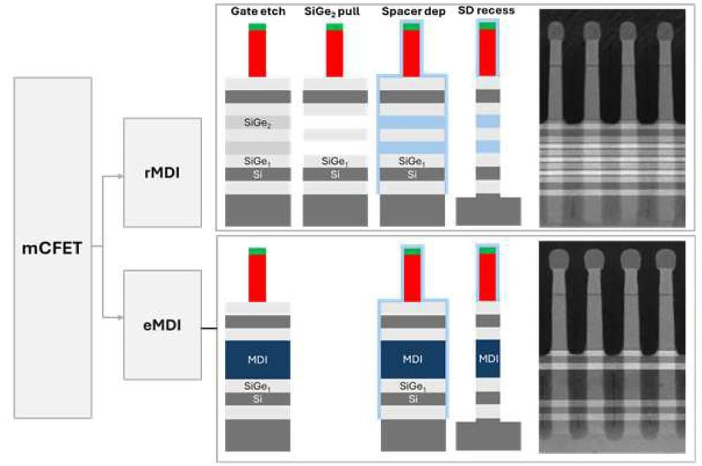
Figure 8 – Comparison of the eMDI and rMDI integration approaches (as presented at IEDM 2025).
The main difference between both approaches is the initial substrate engineering. In the eMDI case, mCFET processing starts from an advanced, bonded substrate with the MDI module already embedded. The use of separate wafers for growing the n- and pMOS active epi stacks prior to the bonding for the first time allows to integrate heterogeneous channels, optimized for maximum n- and pMOS performance. These can be channels with different orientations – as demonstrated in this study – but also, channels with different strain, and even different materials for n and p.
Other advantages include reduced process complexity and simpler epi steps: eMDI avoids the deposition of the complex Si/SiGe1/SiGe2 multilayer stack and the replacement of the dummy SiGe2 layers with a dielectric. Also, by growing the epi stacks on two separate wafers, more Si channels can be included before layer relaxation is reached during epi growth – increasing flexibility in design. The novel MDI module can be integrated into any mCFET baseline, with minor modifications to the mCFET flow.
Outlook: different channel materials, embedded bottom dielectric isolation module
Imec is currently optimizing the critical modules of the eMDI-based mCFET flow with different channel orientations. Future work will extend the proposed scheme to integrate different channel materials for n and p, i.e., Ge for pMOS and Si for nMOS.
In addition, the imec CFET team intends to use a similar ‘embedded’ approach to integrate the bottom dielectric isolation (BDI), a process module that is needed to isolate the S/D epi from the substrate. Using an eBDI approach relying on layer transfer by wafer bonding is expected to facilitate the integration of the backside connection, compared to today’s replacement BDI (rBDI) counterpart. In addition, the eBDI approach will allow more freedom of choice for the BDI material. One option is to use a high thermal conducting material, which may alleviate concerns about the thermal reliability of mCFETs.

Figure 9 – Advanced substrate options for mCFET, with eMDI and eBDI module options.
Conclusion
Imec has identified through a DTCO study the performance boosters that are needed to support aggressive area scaling of mCFET device architectures across multiple technology nodes. While minimizing parasitic gate capacitance is essential for the A7 node, the A5 and A3 nodes will see the introduction of the outer wall forksheet with omega-shaped gate, and an M0 power rail. For A3, additionally introducing heterogeneous channels optimized for p- and nMOS separately will be crucial to maintain performance and power density at ultimately scaled standard cell dimensions. An eMDI module is the key enabling technology for integrating heterogeneous channels in a mCFET flow. This was demonstrated experimentally on mCFET devices with different channel orientations for nMOS and pMOS top devices.
This work has been enabled in part by the NanoIC pilot line. The acquisition and operation are jointly funded by the Chips Joint Undertaking, through the European Union’s Digital Europe (101183266) and Horizon Europe programs (101183277), as well as by the participating states Belgium (Flanders), France, Germany, Finland, Ireland and Romania. For more information, visit nanoic-project.eu.
This article was originally published in Semiconductor Digest.
'반도체 소자 > CFET' 카테고리의 다른 글
| 외벽 포크시트 (0) | 2026.06.10 |
|---|---|
| Complementary FET (CFET) (0) | 2026.06.09 |

댓글